Reliability of Ceramic Substrate
Ceramic PCB (Ceramic Substrate) refers to a special process plate where copper foil is directly bonded to the surface (single or double) of alumina (Al2O3) or aluminum nitride (AlN) ceramic substrate at high temperature. The ultra-thin composite substrate has excellent electrical insulation performance, high thermal conductivity, excellent soldering and high adhesion strength, and can be etched into a variety of graphics like PCB board, with great current carrying capacity. Therefore, the ceramic substrate has become the basic material of high-power electronic circuit structure technology and interconnect technology, which is suitable for products with high caloric value (high-brightness LED, solar energy), and its excellent weather resistance can be applied to harsh outdoor environments.

Main application products: high power LED carrier board, LED lights, LED street lights, solar inverter
Ceramic substrate features:
Structure: Excellent mechanical strength, low warping, thermal expansion coefficient close to silicon wafer (aluminum nitride), high hardness, good processability, high dimensional accuracy
Climate: Suitable for high temperature and humidity environment, high thermal conductivity, good heat resistance, corrosion and wear resistance, UV& yellowing resistance
Chemistry: Lead-free, non-toxic, good chemical stability
Electrical: high insulation resistance, easy metallization, circuit graphics and strong adhesion
Market: Abundant materials (clay, aluminum), easy to manufacture, low price
PCB material thermal characteristics comparison (conductivity) :
Glass fiber board (traditional PCB) : 0.5W/mK, aluminum substrate: 1~2.2W/mK, ceramic substrate: 24[alumina]~170[aluminum nitride]W/mK
Material heat transfer coefficient (unit W/mK) :
Resin: 0.5, alumina: 20-40, silicon carbide: 160, aluminum: 170, aluminum nitride: 220, copper: 380, diamond: 600
Ceramic substrate process classification:
According to the line ceramic substrate process is divided into: thin film, thick film, low temperature co-fired multi-layer ceramic (LTCC)
Thin Film Process (DPC) : Precise control of component circuit design (line width and film thickness)
Thick film process (Thick film) : to provide heat dissipation and weather conditions
Low temperature co-fired multilayer ceramic (HTCC) : The use of glass ceramics with low sintering temperature, low melting point, high conductivity of precious metal co-fired characteristics, multi-layer ceramic substrate) and assembly.
Low temperature co-fired multilayer ceramics (LTCC) : Stack several ceramic substrates and embed passive components and other ics
Thin film ceramic substrate process:
· Pretreatment → sputtering → photoresistance coating → exposure development → line plating → film removal
· Lamination → hot pressing → degreasing → substrate firing → circuit pattern formation → circuit firing
· Lamination → surface printed circuit pattern → hot pressing → degreasing → co-firing
· Printed circuit graphics → lamination → hot pressing → degreasing → co-firing
Ceramic substrate reliability test conditions:
Ceramic substrate high temperature operation: 85℃
Ceramic substrate low temperature operation: -40℃
Ceramic substrate cold and thermal shock:
1. 155℃(15min)←→-55℃(15min)/300cycle
2. 85 ℃ (30 min) please - - 40 ℃ (30 min)/RAMP: 10 min (12.5 ℃ / min) / 5 cycle
Ceramic substrate adhesion: Stick to the surface of the board with 3M#600 tape. After 30 seconds, tear quickly in a 90° direction with the surface of the board.
Ceramic substrate red ink experiment: Boil for one hour, impermeable
Test equipment:
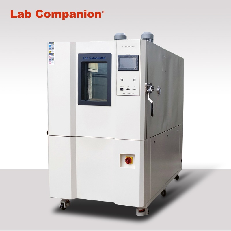
1.High and low temperature humid heat test chamber
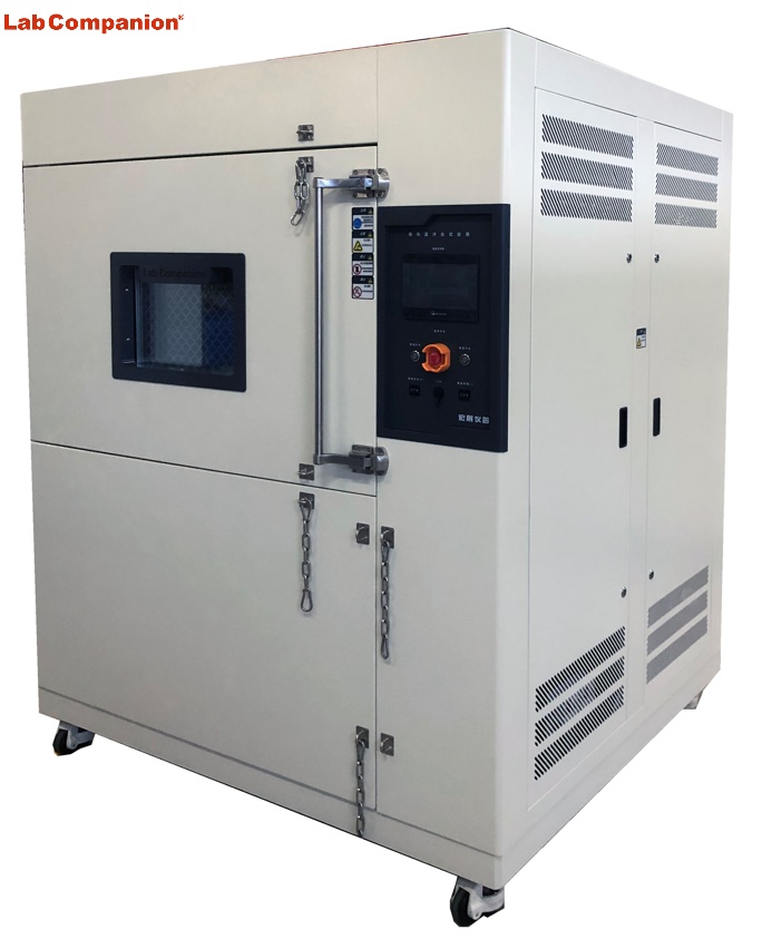
2. Three-box gas type cold and heat shock test chamber


